DIGISYN DL-08/16/32 AES67 Module
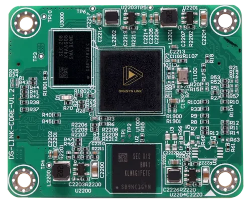
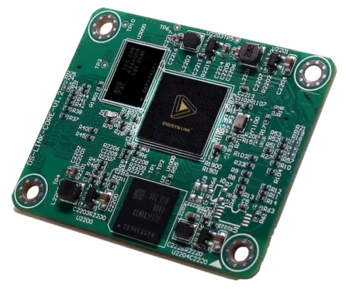
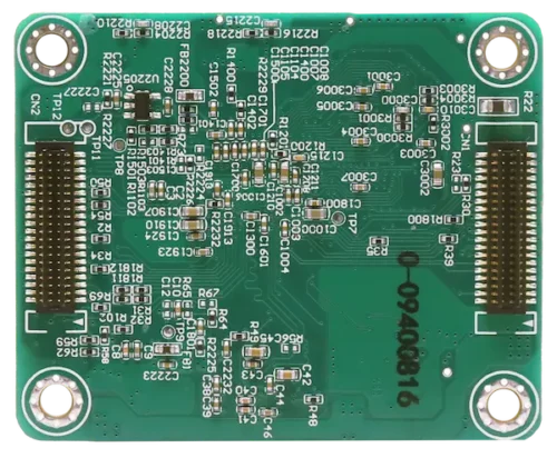
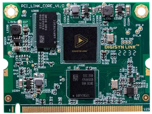
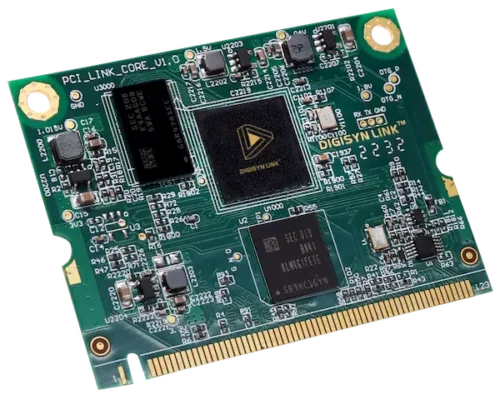
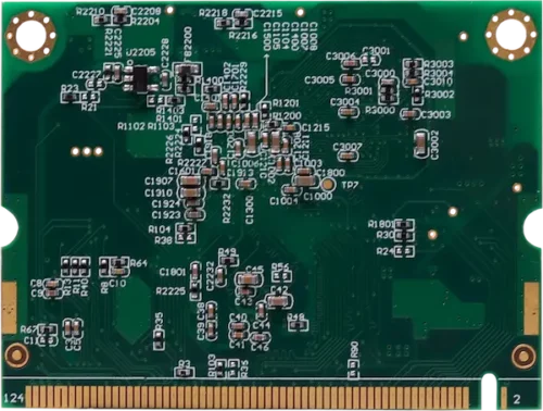
DL-08 Module series
The DL-08/DL-16/DL-32 series presents high-quality AES67+DSP network modules with up to 8x8, 16x16, or 32x32 channels. Featuring ultra-low latency and supporting various sampling rates, these modules offer exceptional audio transmission capabilities. With optional powerful DSP functions and seamless integration into existing setups, the DL-08 series provides an ideal solution for professional audio applications. Ideal for environments requiring advanced audio processing and networking, the DL-08 series is perfect for intgrating in mixing consoles, audio matrices, DSP processors and more.
Mixing Console
Speaker
Audio Matrix
DSP Processor
Amplifier
DIGISYN DL-08/16/32 Specification
| Audio Capabilities | |
| Sampling Rates | 48 / 96 / 192kHz |
| Audio Channels In/Out (48kHz) | Up to 32 x 32 channels |
| Audio Channels In/Out (96kHz) | Up to 8 x 8 channels |
| Audio Channels In/Out (192kHz) | Up to 8 x 8 channels |
| Audio Flows In/Out | Up to 32 x 32 simultaneous streams |
| Digital Audio Format | TDM / I2S |
| Audio Transport Format | AES67 RTP / DIGISYN LINK Network / RAVENNA Network |
| Sample Bit Depth | 32bit / 24bit / 16bit |
| Clocking | Onboard clock |
| DSP Function | PEQ / Delay / Mixer / AFC / Crossover / FIR filter , etc |
| Hardware Parameters | |
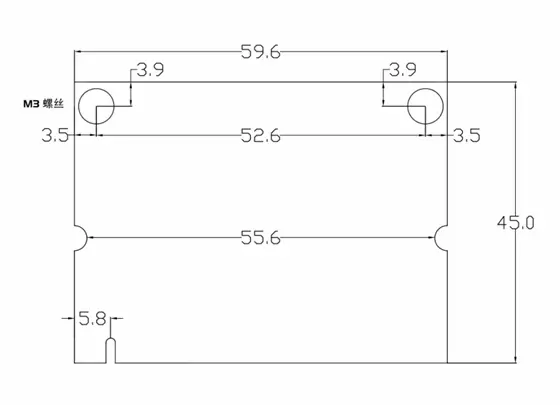
| Form Factor | 45 mm x 55 mm |
| Clock | High quality / Low jitter |
| Physical Connector | Mini-PCI / BTB connector |
| Power | 5V DC 2W |
| Interface | |
| Control Interfaces | SPI / GPIO / UART |
| Network | RMII |
DIGISYN DL-08/16/32 (BTB) PIN Diagram
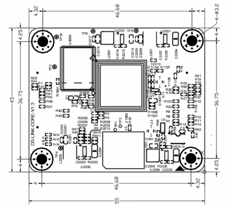
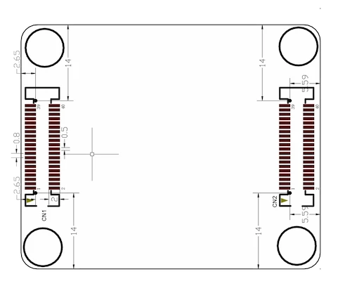
| CN1 | Pin Name | Description | CN2 | Pin Name | Description |
|---|---|---|---|---|---|
| 1:01 | NC | UART1 TX, reserve for future use | 2:01 | I2S0_SDI2 | I2S0 data in |
| 1:02 | NC | UART1 RX, reserve for future use | 2:02 | I2S0_SDI3 | I2S0 data in |
| 1:03 | RMII_RXD1 | RMII Interface | 2:03 | I2S0_SDO0 | I2S0 data out |
| 1:04 | RMII_RXD0 | RMII Interface | 2:04 | I2S0_SDI0 | I2S0 data in |
| 1:05 | RMII_TXD0 | RMII Interface | 2:05 | NC | Test Pin |
| 1:06 | RMII_RXDV | RMII Interface | 2:06 | NC | Test Pin |
| 1:07 | RMII_TXEN | RMII Interface | 2:07 | I2S0_SDO1 | I2S0 data out |
| 1:08 | RMII_TXD1 | RMII Interface | 2:08 | I2S0_SDI1 | I2S0 data in |
| 1:09 | NC | RMII_RXER, reserve for future use | 2:09 | NC | UART0 TX, reserve for future use |
| 1:10 | PHY_MDC | PHY Serial Management Interface | 2:10 | GND | GND |
| 1:11 | RMII_CLK | RMII Interface | 2:11 | I2S0_SDO2 | I2S0 data out |
| 1:12 | PHY_MDIO | PHY Serial Management Interface | 2:12 | I2S0_MCLK | I2S0 MCLK out, module is master |
| 1:13 | GND | GND | 2:13 | GND | GND |
| 1:14 | TDM1_SDO4 | TDM1_SDO4 | 2:14 | GND | GND |
| 1:15 | NC | Test Pin | 2:15 | NC | Test Pin |
| 1:16 | GND | GND | 2:16 | I2S0_LRCK | I2S0 LRCK out, module is master |
| 1:17 | GND | GND | 2:17 | NC | UART0 RX, reserve for future use |
| 1:18 | NC | TDM1_SCLK, reserve for future use | 2:18 | GND | GDN |
| 1:19 | NC | TDM1_LRCK, reserve for future use | 2:19 | I2S0_SCLK | I2S0 SCLK out, module is master |
| 1:20 | GND | GND | 2:20 | I2S0_SDO3 | I2S0 data out |
| 1:21 | GND | GND | 2:21 | GND | GDN |
| 1:22 | NC | Test Pin | 2:22 | UART4 TX | UART4 TX, for module config |
| 1:23 | NC | TDM1 I2S/TDM Data In or Out, reserve for future use | 2:23 | NC | RMII_INT, reserve for future use |
| 1:24 | GND | GND | 2:24 | UART4 RX | UART4 RX, for module config |
| 1:25 | NC | TDM1_SDO1, reserve for future use | 2:25 | NC | Test Pin |
| 1:26 | TDM1_MCLK | TDM1_MCLK, must connect with I2S0_MCLK | 2:26 | NC | Test Pin |
| 1:27 | TDM1_SDI4 | TDM1_SDI4 | 2:27 | GND | GND |
| 1:28 | GND | GND | 2:28 | NC | Test Pin |
| 1:29 | NC | SPI MISO, reserve for future use | 2:29 | NC | Test Pin |
| 1:30 | NC | TDM1_SDI1, reserve for future use | 2:30 | GND | GND |
| 1:31 | NC | SPI MOSI, reserve for future use | 2:31 | GND | GND |
| 1:32 | NC | Test Pin | 2:32 | NC | Test Pin |
| 1:33 | NC | Test Pin | 2:33 | NC | UART2 TX, reserve for future use |
| 1:34 | MUTE | Go high level 1 second after RESET,output | 2:34 | NC | UART2 RX, reserve for future use |
| 1:35 | RESET | Go high level after I2S clock,output | 2:35 | NC | Test Pin |
| 1:36 | GND | GND | 2:36 | NC | Test Pin |
| 1:37 | GND | GND | 2:37 | NC | Test Pin |
| 1:38 | VCC5V | Power | 2:38 | NC | Test Pin |
| 1:39 | VCC5V | Power | 2:39 | NC | Test Pin |
| 1:40 | VCC5V | Power | 2:40 | NC | Test Pin |
DIGISYN DL-08/16/32 (Mini-PCI) PIN Diagram
| PIN NO | PIN NAME | Description | PIN NO | PIN NAME | Description |
|---|---|---|---|---|---|
| 1 | VDD | +3V3 | 2 | VDD | +3V3 |
| 3 | NC | 4 | CODEC_RST | reset AD and DA, output | |
| 5 | NC | 6 | AUDIO_MUTE | MUTE_OUTPUT, output | |
| 7 | NC | 8 | NC | ||
| 9 | NC | 10 | NC | ||
| 11 | NC | 12 | SPI_MISO | ||
| 13 | UART3_RX | Not recommended | 14 | SPI_MOSI | |
| 15 | UART3_TX | Not recommended | 16 | SPI_CLK/ | Not recommended |
| 17 | NC | UART1_RX | |||
| 19 | MAC_TXD0 | RMII interfaces | 18 | SPI_CSN/ | Not recommended |
| 21 | MAC_TXD1 | RMII interfaces | UART1_TX | ||
| 23 | NC | 20 | NC | ||
| 25 | NC | 22 | NC | ||
| 27 | GND | 24 | I2C1_SCL | ||
| 29 | NC | 26 | I2C1_SDA | ||
| 31 | MAC_TXEN | RMII interfaces | 28 | NC | |
| 33 | GND | 30 | GND | ||
| 35 | NC | 32 | NC | ||
| 37 | GND | 34 | NC | ||
| 39 | NC | 36 | GND | ||
| 41 | GND | 38 | MAC_MDIO | RMII interfaces | |
| 43 | MAC_RXD0 | RMII interfaces | 40 | MAC_MDC | RMII interfaces |
| 45 | MAC_RXD1 | RMII interfaces | 42 | MAC_INT | RMII interfaces |
| 47 | NC | 44 | GND | ||
| 49 | NC | 46 | NC | ||
| 51 | GND | 48 | NC | ||
| 53 | MAC_RXDV | RMII interfaces | 50 | NC | |
| 55 | MAC_RXER | RMII interfaces | 52 | NC | |
| 57 | GND | 54 | NC | ||
| 59 | MAC_CLK | RMII interfaces | 56 | NC | |
| 61 | GND | 58 | GND | ||
| 63 | GND | 60 | PHY_RST | Output | |
| 65 | NC | 62 | GND | ||
| 67 | NC | 64 | NC | ||
| 69 | NC | 66 | GND | ||
| 71 | GND | 68 | NC | ||
| 73 | UART4_RX | default, input | 70 | I2S_SCLK | I2S/TDM Serial Clock |
| 75 | UART4_TX | default, output | 72 | GND | |
| 77 | GND | 74 | NC | ||
| 79 | NC | 76 | I2S_MCLK | I2S/TDM Master Clock | |
| 81 | GND | 78 | GND | ||
| 83 | GND | 80 | NC | ||
| 85 | I2S_SDO0 | I2S Serial Data Output0 | 82 | I2S_LRCK | I2S/TDM Left/Right Clock |
| 87 | I2S_SDO1 | I2S Serial Data Output1 | 84 | GND | |
| 89 | I2S_SDO2 | I2S Serial Data Output2 | 86 | NC | |
| 91 | I2S_SDO3 | I2S Serial Data Output3 | 88 | NC | |
| 93 | GND | 90 | NC | ||
| 95 | I2S_SDO4 | I2S Serial Data Output4 | 92 | NC | |
| 97 | I2S_SDO5/ | I2S Serial Data Output5 | 94 | GND | |
| I2S_SDI7 | 96 | USB_OTG_ID | |||
| 99 | I2S_SDO6/ | I2S Serial Data Output6 | 98 | USB_OTG_D_N | |
| I2S_SDI6 | 100 | USB_OTG_D_P | |||
| 101 | I2S_SDO7/ | I2S Serial Data Output7 | 102 | GND | |
| I2S_SDI5 | 104 | NC | |||
| 103 | GND | 106 | NC | ||
| 105 | I2S_SDI0 | I2S Serial Data Input0 | 108 | NC | |
| 107 | I2S_SDI1 | I2S Serial Data Input1 | 110 | NC | |
| 109 | I2S_SDI2 | I2S Serial Data Input2 | 112 | GND | |
| 111 | I2S_SDI3 | I2S Serial Data Input3 | 114 | +3V3 | |
| 113 | GND | 116 | VDD | +3V3 | |
| 115 | I2S_SDI4 | I2S Serial Data Input4 | 118 | VDD | +3V3 |
| 117 | I2S_SDO7/ | I2S Serial Data Input5 | 120 | VDD | +3V3 |
| I2S_SDI5 | 122 | VDD | +3V3 | ||
| 119 | I2S_SDO6/ | I2S Serial Data Input6 | 124 | NC | |
| I2S_SDI6 | |||||
| 121 | I2S_SDO5/ | I2S Serial Data Input7 | |||
| I2S_SDI7 | |||||
| 123 | NC |